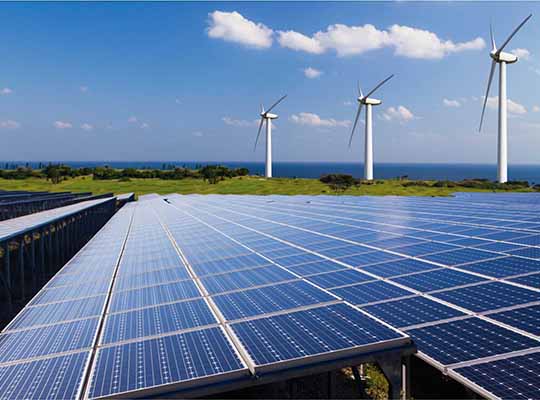
Today, some 85 percent of installed photovoltaic (PV) cells are manufactured from silicon, as it’s both particularly suited to turning light into electricity and plentiful. Too, PV cells can be produced in volume by adopting wafer manufacturing techniques pioneered by the Integrated Circuit (IC) industry. However, silicon has some downsides, including a maximum efficiency of around 33 percent, energy-intensive high temperature processing, and fragility.
Alternative PV technologies using new materials, architectures, and assembly techniques have been developed to address silicon’s drawbacks. New materials include the compound semiconductors gallium arsenide (GaAs) and gallium phosphide (GaP), as well as the mineral perovskite (CaTiO). The new energy-focusing Concentrated PV (CPV) architecture and assembly techniques use multi-junction, thin-film, and large crystals for high energy efficiency and durability.
While silicon PV cells are likely to dominate large-scale electricity generation due to mass production and falling prices, alternative technologies will find use in niche applications. One such application is wireless IoT sensors where efficient, compact, durable, and inexpensive PV technology could harvest solar energy to charge device batteries. Such technology would be a boon for the Internet of Things (IoT) roll-out because it would enable wireless sensors to operate reliably with little or no maintenance.
This article explores how PV cells work, the role of silicon, and the advantages and disadvantages of silicon as the underlying semiconductor, as well as the potential of new semiconductors, architectures, and assembly techniques.
Photovoltaic Process
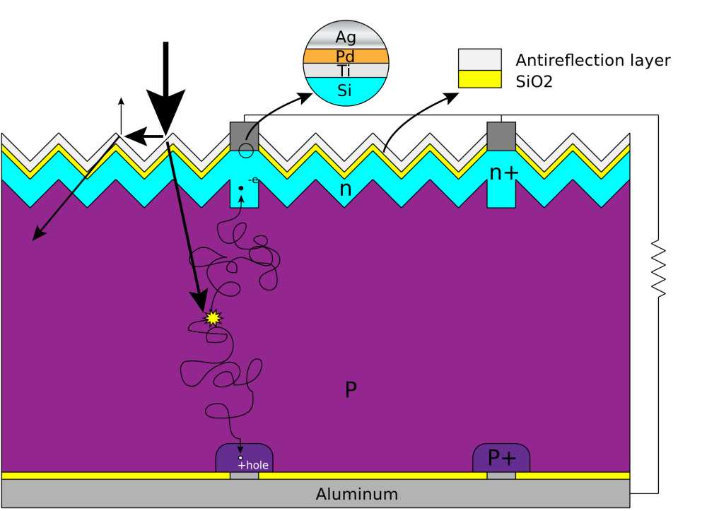
Although a deep understanding of the photovoltaic (also called photoelectric) process requires familiarity with quantum mechanics, the basic principles of PV cell operation are relatively straightforward: PV cells take advantage of semiconductor p-n junctions. In the n-type material, electrons act as current carriers, with electron vacancies or “holes” doing the same job on the p side of the junction.
When a photon within a narrow band of wavelengths enters the semiconductor crystal matrix, there is some probability that it will be absorbed by an electron bound to an atom in the n-type material, endowing the particle with sufficient energy to escape from its parent atom. The excess electrons on the n-type side of the junction then diffuse across the junction to recombine with holes on the p-type side, creating a potential difference across the joint. The incorporation of a conducting return path between the two sides of the joint allows a Direct Current (DC) to flow (Figure 1).
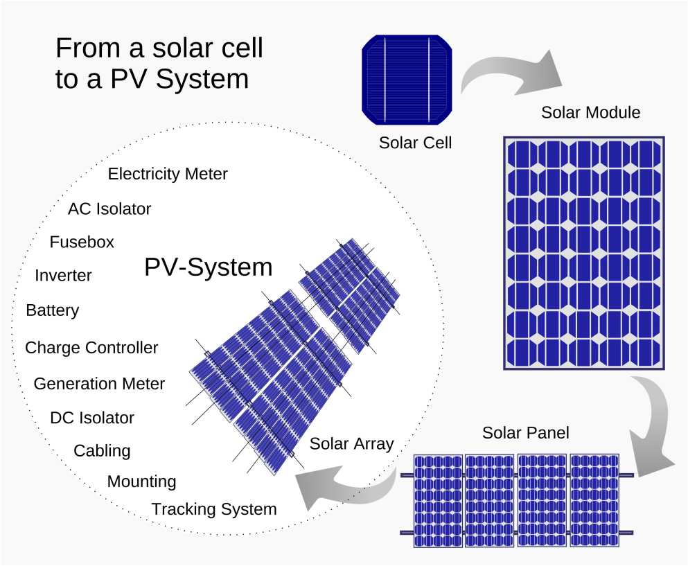
As a PV cell is made up of thousands of these p-n junctions, the generated current is multiplied. In the commercial products, these cells are combined to form modules and ultimately create panels. The DC voltage can be turned into AC by an inverter to do useful work or send power directly to the distribution grid (Figure 2).
First Generation PV Cells: Single-Junction Silicon
First-generation PV panels are largely fabricated from a crystalline form of silicon (“c-Si”). The key drivers for silicon’s large uptake is its PV performance and convenience of supply. The bulk material is plentiful (making up 28 percent of the Earth’s crust), and the techniques and facilities for manufacture have been borrowed from the chip industry. However, processing the large-scale silicon wafers for PV panels is energy intensive, complex, and expensive.
Cost has been mitigated in part due to excess global manufacturing capacity; the price of silicon PV panels has declined by around 30 percent in the last year alone. Government subsidies designed to encourage the uptake of silicon PV panels to reduce reliance on fossil fuels for electricity generation have also played their part in encouraging adoption. Nonetheless, the technology remains too costly for many niche applications.
Silicon Advantages: Efficiency And Band Gap
Silicon offers several advantages for PV technology. First, its PV efficiency is good. (Efficiency, in this case, refers to the ratio of sunlight received by a PV cell to the energy it generates. Averaged out over the surface of the planet, the Sun delivers around 1100W/m2 when directly overhead. A PV panel measuring 1m2 exposed to this level of sunlight and exhibiting 10 percent efficiency, for example, will output around 110W.
The key characteristic that limits a semiconductor’s maximum efficiency is its band gap. The band gap is the amount of energy required to liberate an electron from an atom into the “conduction band” and is measured in electron volts (eV); 1eV is approximately equal to 1.602×10⁻¹⁹J.
The energy of photons is determined by their wavelength, with photons of a shorter wavelength (higher frequency) being more energetic. Many sunlight photons entering a c-Si lattice will carry insufficient energy to liberate an electron and will therefore do little more than heat up the material. Photons with greater energy than that required to bridge the band gap might liberate a single electron, but their excess energy will again just contribute to heating up the crystal rather than doing anything useful.
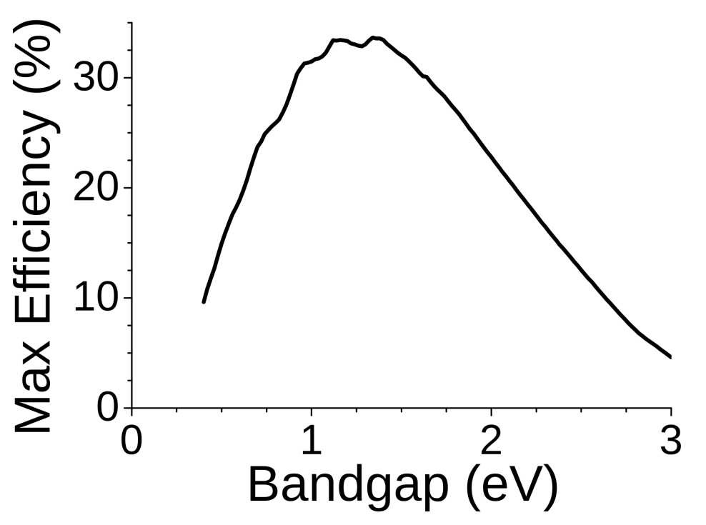
In 1961, William Shockley and Hans-Joachim Queisser calculated the theoretical maximum PV efficiency for single-junction (cells made of just one semiconductor) PV cells across a range of band gaps (Figure 3). The calculation revealed that the optimum band gap for a single-junction PV cell was 1.13eV, which yielded a maximum efficiency of around 33 percent. It turns out that silicon’s band gap of 1.10eV is close to the optimum figure.
Silicon Drawbacks: Crystal Size, Energy, Efficiency, And Fragility
Silicon as a material is not perfect for PV cells, however. For example, band gap is not the only determinant of efficiency; crystal size also has a major effect. If a material is made up of small crystals, electron mobility is reduced by the large number of crystal interfaces. Reduced mobility restricts current flow and, in turn, efficiency.
Additionally, these drawbacks further hinder silicon as an ideal semiconductor for PV cells:
- Maximum theoretical efficiency is just 33 percent. The best commercial c-Si PV panels achieve around 24 percent efficiency in practice wasting over three-quarters of the sun’s energy.
- Fragility, requiring mechanical support from heavy glass panels, adding weight and cost.
- Energy-intensive, high-temperature, and complex processing.
- Inherently expensive, which could introduce challenges if supply becomes restricted and/or subsidies are withdrawn.
New Developments In PV Technology
In the last several years, second-generation PV products have been commercialized, and third-generation technology has entered the R&D labs. Second- and third-generation technologies look to build on the success of mature silicon technology, particularly the established support infrastructure—such as isolators, meters, controllers, and inverters that are largely independent of the PV technology type—while addressing some of silicon’s drawbacks.
Second-Generation PV Technology
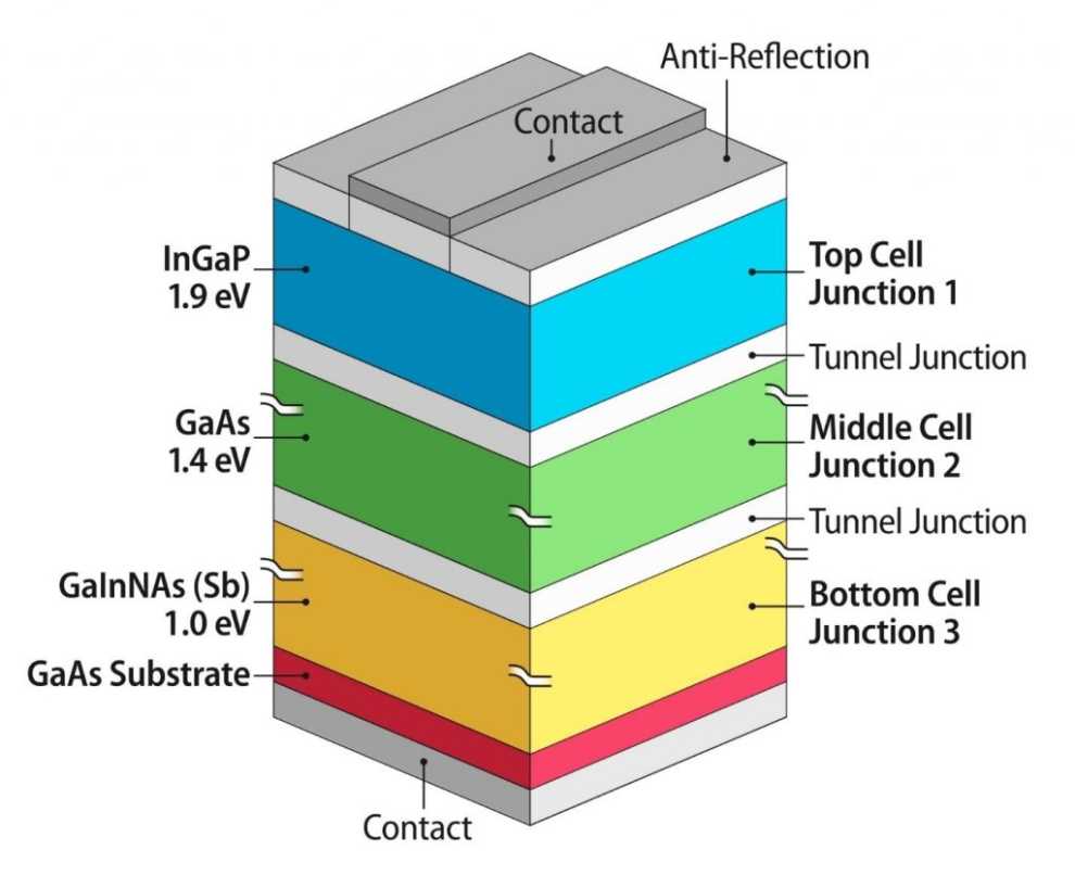
Second-generation PV panels focus on nanometer to micrometer thick layers of PV material mounted on a glass, plastic, or metal substrate. These “thin-film” PV (TFPV) cells (also called “multi-junction” products because of the additional active layers) are cheaper and less energy intensive to manufacture, use less expensive material, are low in weight, and are suited to applications such as semi-transparent, PV glazing material that can be laminated onto windows (Figure 4).
The downside of TFPV panels is that the manufacturing, energy, cost, and weight advantages are traded-off against efficiency. Some of the potential efficiency gains of bulk material multi-junction PV panels is lost because the thin films comprise tiny crystals that affect electron mobility. Instead of c-Si, for example, which comprises comparatively huge crystals, commercial TFPV panels use either polycrystalline silicon (very small crystals) or amorphous silicon (no crystals). TFPV panels promise efficiencies of 20 percent although today’s commercial products typically operate at 10 percent efficiency.
A second disadvantage of TFPV panels is relatively rapid degradation of the thin films reducing the panel lifetime. Second-generation PV cells are unlikely to challenge silicon’s dominance for large-scale electricity generation but offer promise in applications where lower cost, weight, and durability can be traded-off against efficiency.
Third-Generation PV Technologies
PV technology is continually being developed to enhance first- and second-generation technologies. And research into new areas is uncovering technology that will form the foundation of a third generation of PV product. These developments and research generally fall into four sectors:
- Materials: Complementing silicon with semiconductors of different band gaps so that photons of lower energy can liberate electrons and so that those of a higher energy convert more of that energy to electricity.
- Structure: Introducing techniques that lower the energy intensity and complexity of first-generation PV panel production.
- Processing: Improving semiconductor processing techniques to enhance the quality and size of crystals such that electron mobility is raised.
- Mechanical: Amplifying the number of photons that fall on a unit area of substrate by focusing incident light with mirrors or lenses.
Material Developments
Converting more of the incident photon energy into electricity is possible by introducing materials with lower and higher band gaps than silicon. Silicon’s band gap of 1.1eV is the best of any single semiconductor for harvesting energy from visible light. However, much of the energy from the sun is carried by photons with energy below this band gap. For example, while a blue-light photon can carry three times as much energy as a red one, two-thirds of that energy is wasted even if the photon is absorbed by a silicon electron.
Semiconductors with band gaps lower than silicon enable photons that would otherwise be useless to contribute to the PV effect. Indium arsenide (InAs), for example, has a band gap of 0.36eV and has been used successfully to complement silicon.
Semiconductors with higher band gaps than silicon allow more of the energy of shorter wavelength photons to contribute to electricity generation. Materials such as gallium arsenide (GaAs), which has a band gap of 1.43eV, and gallium phosphide (GaP), which has a band gap of 2.25eV, have also been used with success. Several lines of research have resulted in further compounding of these materials—for example, indium gallium arsenide (InGaAs) and indium gallium phosphide (InGaP)—to further optimize the PV effect.
Structural Developments
Alternative band gap semiconductors have a lower maximum efficiency than silicon alone, so there is no benefit in employing them singly. Instead, one or more semiconductors are used together in a multilayer structure. Materials with the largest band gap—requiring short wavelength (high energy) photons to dislodge electrons—are positioned at the top, allowing low energy photons to pass through without interaction to then be absorbed by lower band gap materials in the following layers. Transparent conductors are required at each layer to carry the generated current yet let photons pass through to the lower layers. This technology has been deployed with success in TFPV panels and remains the focus a key area of research.
Silicon has a maximum efficiency of 33 percent, but this figure can theoretically be bettered by multilayer PV panels. A two-layer cell, for example, with one layer featuring a band gap of 1.64 and the other 0.94eV, could reach a maximum efficiency of 44 percent. Similarly, a three-layer PV cell with band gaps of 1.83, 1.16, and 0.71eV, would have a maximum theoretical efficiency of 48 percent. Commercial multilayer products comprise two, three, or four layers.
Processing Developments
Researchers are investigating new groups of materials for third-generation PV panels that combine the high efficiencies of the first generation with the simpler and cheaper manufacturing of the second.
One group of materials that has caused much excitement is derived from the mineral perovskite (CaTiO). The group of materials has band gaps ranging from 1.4 to 2.5eV. The theoretical maximum efficiency of the perovskite group can’t match silicon, but recent rapid efficiency gains from around 4 to 20 percent have raised hope that commercial products will eventually be more efficient than TFPV panels.
The key advantage of the perovskite group over silicon is the comparative ease and low processing temperatures with which millimeter-sized perfect crystals can be grown. This is a huge size for a perfect crystal lattice, and it dramatically increases electron mobility and hence efficiency while slashing manufacturing costs. Current lines of research are aimed at growing even larger perfect crystals; for example, researchers at MIT in the U.S. have recently discovered how to “heal” crystal defects in a perovskite-based PV cell by exposing the cell to intense light.
Elsewhere, researchers at University of California, Berkeley have discovered that different facets of the perovskite crystals have markedly different efficiencies. The scientists are now focusing their research on ways of processing the bulk material such that only the most efficient facets interface with the PV cell electrodes as a method of boosting overall efficiency.
As with TFPV materials, a key challenge currently limiting the commercial deployment of perovskite-based PV cells is the speed at which the material degrades.
Mechanical Development
Another development objective for third-generation PV panels is Concentrated PV (CPV) technology. CPV is designed to focus sunlight using lenses and mirrors such that a dramatically higher number of photons fall on a unit area of PV panel. The technique typically employs high-efficiency, multi-junction PV cells constructed, as shown in Figure 4. Focusing the light increases efficiency, enabling dramatic reductions in panel size, lowering the cost and weight of the product, and increasing the number of locations where it can be installed.
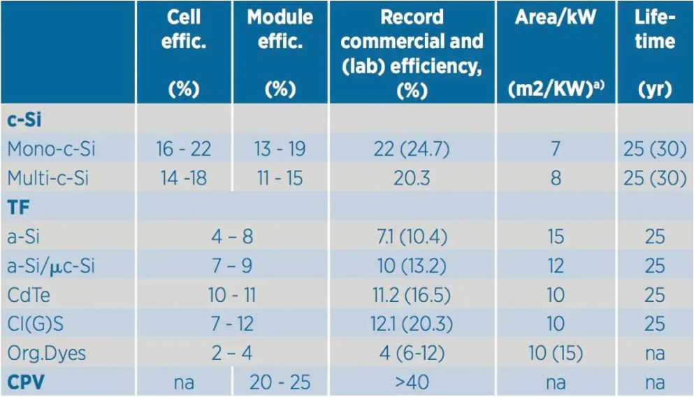
“Low” CPV focuses the equivalent of two to 100x sunlight onto the panel, while “high” CPV can multiply the light to the equivalent of 1000x sunlight. CPV systems often use solar trackers and sometimes a cooling system to increase efficiency. Table 1 summarizes the efficiency of current PV cell technology.
Case Study: Energy-Harvesting Wireless IoT Sensors
The key application for PV technology is for renewable-energy generating capacity to feed the electricity grid. But third-generation technologies—which promise less expensive, more durable, and smaller PV panels—promise to introduce energy-harvesting niche applications.
Wireless IoT Sensors
Designers of IoT wireless sensors have long been keen to take advantage of energy harvesting. It is envisaged that the IoT will comprise billions of sensors with many positioned remotely and therefore isolated from main power and difficult to access for maintenance such as battery changes.
Many of the products will employ low-power wireless technologies such as Bluetooth low energy and zigbee, which have been designed from the ground up to run from modest power resources. Many applications are powered from compact primary cells with capacities around 220mAh. In low-duty cycle operation, the average current draw from a low-power wireless System-on-Chip (SoC) is in the microampere range, extending battery life to thousands of hours (several months) of operation.
However, extending battery life by replacing a primary battery with a secondary battery and recharging via a PV cell extends self-contained operation to several years.
Energy-Harvesting Technology
Energy harvesting technology for small-capacity, Li-ion cell charging is a proven technology. For example, Mikroe’s energy-harvesting module is a silicon PV cell capable of producing up to 0.4W at 4V.
The voltage and current from a PV cell varies considerably. As such, the voltage/current output must be regulated for Li-ion battery charging, as Li-ion batteries require careful current/voltage management during the charging cycle.) Purpose-designed, highly-integrated power management chips are available for the job.
For example, Maxim’s MAX17710 power management IC can manage poorly-regulated sources such as PV cells with output levels ranging from 1µW to 100mW. The device also includes a boost regulator circuit for charging the battery from a source as low as 0.75V. An internal regulator protects the cell from overcharging. 3.3, 2.3, or 1.8V outputs are supplied to the wireless IoT sensor via a Low-Dropout (LDO) linear regulator.
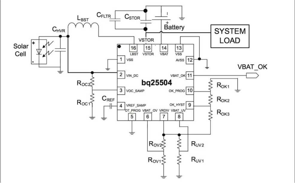
Texas Instruments also offers a power management IC, the bq25504.The device is specifically designed to efficiently acquire and manage power generated from PV cells. The chip integrates a DC-DC boost converter/charger that requires only microwatts of power and a voltage as low 330mV to commence energy harvesting (Figure 5).
Third-Generation PV Technology Applied
While current PV cell energy-harvesting solutions work satisfactorily, they do have some downsides. For example, Mikroe’s energy-harvesting module measures 7 x 6.5 x 0.3cm (a surface area of 45.5cm2), is relatively heavy and fragile. However, silicon PV cells like this product are currently the only practical choice because of their efficiency compared with alternatives.
Third-generation cells incorporate technology to boost efficiency beyond the current 10 percent enjoyed by commercial products. Technologies currently in the lab are projected to double efficiency in the next several years; that would introduce silicon PV cell-type performance to TFPV cells combined with advantages of lower cost, light weight, and greater robustness.
A third-generation TFPV cell measuring just 4cm2 in direct sunlight, for example, would receive around 0.22W incident power. At 20 percent efficiency, the TFPV cell would output around 44mW. While charging at an average of 3.5V (voltage varies during a Li-ion battery charging cycle), the current supplied from the power management chip would be around 12mA, sufficient to fully recharge a 300mAh Li-ion battery in around 25 hours.
While such a charging regime would take several days of full sunshine, note that the Li-ion battery will only discharge at a rate of a perhaps a few mAh per day under typical low power wireless sensor operation, requiring the PV cell to only top-up the battery (rather that fully charge) ensuring it can easily cope with the energy demand even on days without full sunshine.
Compact third-generation PV cells are yet to be commercialized. And when mass production does commence, prices are likely to initially be too high for wireless IoT sensor applications. However, as the technology matures and demand increases, TFPV cells will become much cheaper and a practical proposition for this niche application.
Simultaneously, the efficiency of TFPV PV cells will continue to increase, bringing greater advantages to energy-harvesting wireless sensor designs including:
- Energy harvesting from artificial light for indoor sensors.
- Reduction in panel size for given power output for highly space-constrained designs.
- More power available to run complex software algorithms on advanced wireless SoCs.
- Increased wireless sensor range and throughput.
- Multiple sensors powered from a single PV panel.
Conclusion
An estimated 85 percent photovoltaic (PV) cells currently installed are manufactured from silicon, as it’s both plentiful and suited to turning light into electricity. Second- and third- generation PV technologies are addressing silicon’s downsides that include a maximum efficiency of only about 33 percent, energy-intensive high temperature processing, and fragility.
Second-generation PV panels focus “thin-film” PV cells that are mounted on a glass, plastic, or metal substrate. These are cheaper and less energy intensive to manufacture, use less expensive material, are low in weight, and are suited to applications such as semi-transparent, PV glazing material that can be laminated onto windows. These are unlikely to challenge silicon’s dominance for large-scale electricity generation but offer promise in applications where lower cost, weight, and durability can be traded-off against efficiency.
Third-generation PV cells promise even more by matching the efficiency of silicon while building on the advantages of second-generation products. This will make the cells a good option for remote, low-maintenance IoT sensor applications using rechargeable Li-ion batteries continually replenished by the sun’s energy. These PV technologies use new materials, structure, processing, and mechanical techniques to address silicon’s drawbacks. New materials include the compound semiconductors gallium arsenide (GaAs) and gallium phosphide (GaP), as well as the mineral perovskite (CaTiO); the new
energy-focusing Concentrated PV (CPV) architecture and assembly techniques use using multi-junction, thin-film, and large crystals for high energy efficiency and durability.
Niche applications like energy-harvesting wireless IoT sensors, which require efficient, compact, durable, and inexpensive PV technology, stand to benefit from third-generation PV cells. Such technology would enable wireless sensors to operate reliably with little or no maintenance. As third-generation PV technologies evolve, we can expect to see additional wireless sensor designs, such as harvesting energy from indoor lighting and other applications that require compact, efficient, powerful, and robust designs.
Key Takeaways
- Silicon is the market-leading material for general-purpose PV panel applications because the raw material is plentiful, manufacturing infrastructure is established, and if offers high efficiency.
- Silicon PV cells have some notable downsides: They are heavy, fragile, energy intensive to produce, and expensive.
- This makes silicon impractical for energy harvesting applications for compact wireless IoT sensors.
- New materials and PV cell construction techniques address silicon’s drawbacks, but lower efficiency limits usefulness for wireless IoT sensors.
- Third-generation cells’ improved efficiency will make the technology suitable for wireless IoT sensors, and promises to increase computational power, wireless range, and throughput at an affordable cost.
About The author:
Steven Keeping is a contributing writer for Mouser Electronics and gained a BEng (Hons.) degree at Brighton University, U.K., before working in the electronics divisions of Eurotherm and BOC for seven years. He then joined Electronic Production magazine and subsequently spent 13 years in senior editorial and publishing roles on electronics manufacturing, test, and design titles including What’s New in Electronics and Australian Electronics Engineering for Trinity Mirror, CMP and RBI in the U.K. and Australia. In 2006, Steven became a freelance journalist specializing in electronics. He is based in Sydney.