KEIHIN RAMTECH will attend SVC TechCon2023 in Washington, D.C.
As part of the fight against global warming concerns, energy sources that do not rely on fossil fuels are major subjects. Expectations for solar cells are also high. Perovskite solar cells (PSC), which have attracted particular attention, are in particularly high demand in the market and are attracting attention as next-generation solar cells. Perovskite is a device structure consisting of very delicate organic layers in cells, and conventional technologies using dry process sputtering methods cause damage to the transparent conductive oxide (TCO) film when deposited, resulting in degradation of the organic layers, which prevents the desired device characteristics from being achieved. It has been difficult to use sputter deposition for TCO.
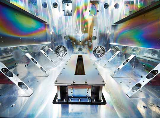
Advantages of RAM FORCE Sputtering
Improved sputtering deposition characteristics for perovskite solar cells
RAM FORCE, which has a unique structure by four facing targets and magnetic field arrangement have realized low-damage deposition, and in the case of TCO deposition on PSC, the carrier lifetime, which is a guideline for damage, has been improved by about 30% compared to planar sputtering equipment. The low-damage property has been utilized to achieve low-damage deposition. By taking advantage of the low-damage sputtering characteristics, the PSC achieves a Fill Factor (FF) of more than 75%, which is a curve factor representing cell characteristics. It has begun to be used in R&D applications and pilot lines.
Realization of low-temperature sputtering deposition
RAM FORCE enables a low-temperature deposition at less than 60℃ (ITO: 100 nm), and thus it is applicable to sputtering deposition on flexible substrates.
Future Development of RAM FORCE
RAMTECH is also focusing on other applications. For the hole transport layer (HTL) of PSC, NiOx layer can be used instead of the currently used organic layer such as Spiro-OMeTAD to realize low-damage sputter deposition and low resistance. Furthermore, by changing the deposition process conditions, NiOx can also be deposited as the electron transport layer (ETL), making it possible to use the same material for both HTL and ETL deposition, thereby improving characteristics and reducing costs.